
Block Reference
The USRP blockset currently consists of these blocks:
| usrp_sink | The usrp_sink block is used to transfer data from a Simulink model to the USRP. |
| usrp_source | The usrp_source block is used to transfer data from the USRP to a Simulink model. |
| usrp_helper | The usrp_helper block is used to set properties which are common to a sink and a source on the same USRP board, such as the firmware or USB Block Size. |
| Set Bitstream | The Set Bitstream block is used to choose the right FPGA bitstream for the usrp_helper block. |
| Set Firmware | The Set Firmware block is used to choose the right USB firmware for the usrp_helper block. |
| Bitfile Generator | The Bitfile Generator block is used to generate a bitstream for the Altera Cyclone FPGA on the USRP mainboard. |
| FPGA Demos | The FPGA Demos block opens the demo section for the USRP. |
usrp_sink
The usrp_sink block is used to transfer data from a Simulink model to the USRP.
Description
This block consumes a certain number of input streams (depending on how many daughterboards on the USRP are enabled) and sends them out to the USRP.
Dialog Box
The usrp_sink block has "per-block" settings, displayed on the USRP tab pane, and "per-daughterboard" settings, displayed on the Side A and Side B tab panes.
USRP Tab Pane
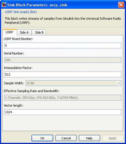
- USRP Board Number
-
Specify on which USRP board this usrp_sink block acts upon. The first USRP board is numbered 0, the second 1 etc.
- Serial Number
-
Informational message stating the USB serial number of the specified USRP board. Read only.
- Interpolation Factor
-
Specifies the interpolation factor which is to be used inside the USRP to bring the baseband sample rate to 128 MSps. Some restrictions apply, depending on the choosen FPGA bitstream. If the interpolation factor could not be set when starting the simulation, check that it is inside the supported range of the FPGA. For some FPGA bitstreams, the interpolation factor must be a multiple of four.
- Sample Width
-
Number of bytes to transfer across the USB bus for one sample. For usrp_sink blocks, 16 bit is the only allowed value.
- Effective Sampling Rate and Bandwidth
-
Displays the effective bandwidth across the USB bus, depending on the number of enabled daughterboards/subdevices and the Sample Width. Read only.
- Vector length
-
Number of samples of one input frame of this block. This number must be calculated in a way such that the block size that goes over the USB bus is a multiple of 512 bytes. That means that the equation
Vector length * 2 * Sample Width/bytes * Number of active channels mod 512 = 0 must be true. The factor 2 comes from complex samples.
Daughterboard Tab Panes ("Side A" and "Side B")
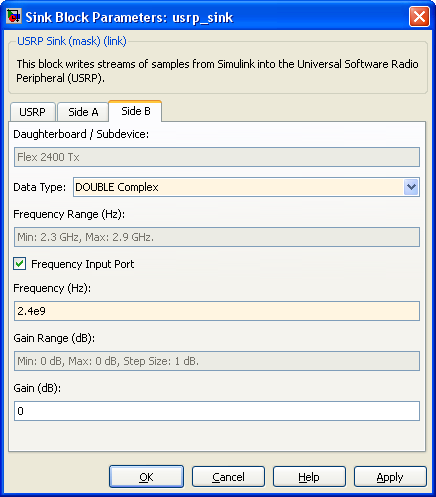
- Daughterboard / Subdevice
-
Displays the type of the daughterboard installed on the USRP. Read only.
- Data Type
-
Enables transmitting with this daughterboard when set to anything different from Disabled. For each daughterboard which is not disabled, one complex-valued input port or two real-valued input ports of the specified data type appear on this Simulink block.
For example, assume that the Data Type of the daughterboard on Side A is set to INT16, and that of Side B is set to SINGLE Complex. This means that input port one of this block expects a stream of real-valued frames, being the in-phase part of the signal going to daughterboard A. Input port two expects the real-valued quadrature part of the same signal. The daughterboard on side B is fed by the complex-valued stream going into port three of this block.
- Frequency Range (Hz)
-
Displays the frequency range that is supported by this daughterboard. Read only.
- Frequency Input Port
-
Enables a frequency input port to tune the seleceted daughterboard during runtime. The port expects a real-valued and sample-based signal of datatype DOUBLE. The sample-time of the input port is defined by the usrp_sink block.
Setting the value Frequency (Hz) is still required for initialization purpose.
- Frequency (Hz)
-
Enter the frequency at which the signal entering this block shall be transmitted with the USRP.
- Gain Range (dB)
-
Displays the gain range supported by this dautherboard. Read only.
- Gain (dB)
-
Enter any gain or attenuation within the gain range of the daughterboard.
usrp_source
The usrp_source block is used to transfer data from the USRP to a Simulink model. To get a connectionto the USRP, the usrp_helper block is mansatory.
Description
This block produces a certain number of output streams (depending on how many subdevices on the daughterboards on the USRP are enabled) by reading data from the USRP.
Dialog Box
The usrp_source block has "per-block" settings, displayed on the USRP tab pane, and "per-subdevice" settings, displayed on the Side A - 1 through Side B - 2 tab panes.
USRP Tab Pane
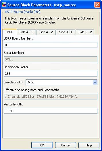
- USRP Board Number
-
Specify on which USRP board this usrp_source block acts upon. The first USRP board is numbered 0, the second 1 etc.
- Serial Number
-
Informational message stating the USB serial number of the specified USRP board. Read only.
- Decimation Factor
-
Specifies the decimation factor which is to be used inside the USRP to bring the ADC sample rate of 64 MSps to the baseband sample rate. Some restrictions apply, depending on the choosen FPGA bitstream. If the decimation factor could not be set when starting the simulation, check that it is inside the supported range of the FPGA. For some FPGA bitstreams, the decimation factor must be even.
- Sample Width
-
Number of bytes to transfer across the USB bus for one sample. Setting this to 8 Bit yields in a higher maximum sample rate across the USB but decreases the dynamic range of the captured signal.
- Effective Sampling Rate and Bandwidth
-
Displays the effective bandwidth across the USB bus, depending on the number of enabled daughterboards/subdevices and the Sample Width. Read only.
- Vector length
-
Number of samples to put into one output frame of this block. This number must be calculated in a way such that the block size that goes over the USB bus is a multiple of 512 bytes. That means that the equation
Vector length * 2 * Sample Width/bytes * Number of active channels mod 512 = 0 must be true. The factor 2 comes from complex samples.
Subdevice Tab Panes ("Side A - 1" through "Side B - 2")
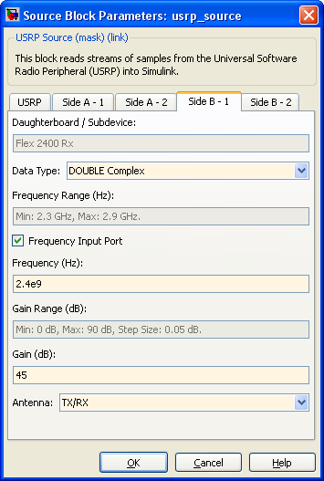
- Daughterboard / Subdevice
-
Displays the type of the daughterboard installed on the USRP. Read only.
- Data Type
-
Enables receiving with this subdevice when set to anything different from Disabled. For each subdevice which is not disabled, one complex-valued output port or two real-valued output ports of the specified data type appear on this Simulink block.
For example, assume that the Data Type of the daughterboard on Side A - 1 is set to INT16, and that of Side B - 1 is set to SINGLE Complex. This means that output port one of this block produces a stream of real-valued frames, being the in-phase part of the signal from subdevice 1 on daughterboard A. Output port two produces the real-valued quadrature part of the same signal. Subdevice 1 on the daughterboard on side B produces one complex-valued stream on port three of this block.
- Frequency Range (Hz)
-
Displays the frequency range that is supported by this daughterboard. Read only.
- Frequency Input Port
-
Enables a frequency input port to tune the seleceted daughterboard during runtime. The port expects a real-valued and sample-based signal of datatype DOUBLE. The sample-time of the input port is defined by the usrp_sink block.
Setting the value Frequency (Hz) is still required for initialization purpose.
- Frequency (Hz)
-
Enter the frequency at which a signal shall be captured.
- Gain Range (dB)
-
Displays the gain range supported by this subdevice. Read only.
- Gain (dB)
-
Enter any gain within the gain range of the daughterboard.
- Antenna
-
Daughterboards with multiple antenna input ports can be configured to use one specified input connnector for the signal. Setting this parameter to a value which is not available on the dautherboard usually produces an error (or has no effect at all, depending on the type of the dautherboard).
The setting I&Q (BasicRX/LFRX only) has a special meaning. The two input connectors on thoses dautherboards are usually mapped to the two subdevices of the dautherboard. If, however, both inputs are fed by the inphase and quadrature parts of the same signal, they both can be combined into one complex signal. In this case, subdevice two can not be used seperately any more. (In fact, this setting chooses subdevice three on those boards.)
The Antenna parameter is only available on the first subdevice of each daughterboard.
usrp_helper
The usrp_helper block is used to set properties which are common to a sink and a source on the same USRP board, such as the firmware or USB Block Size. The block is mandatory for the usrp_sink and usrp_source block.
Description
This block can be placed anywhere into a Simulink model. Other blocks reference it by searching for blocks of type usrp_helper and comparing the parameter usrp_number against their own usrp_number. Parameters that control the operation of USRP boards are Firmware Filename, FPGA Bitstream Filename, USB Block Size and Number of USB Blocks. If this block is not found in a model the default values will be used for the parameters.
This block is a purely virtual block. If the Block Reduction option is enabled on the Optimization pane of the Configuration Parameters dialog box of a model, this block does not execute during simulation. Furthermore, this block does not add a single line of code to files generated by the Real Time Workshop.
Dialog Box
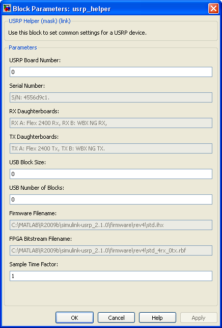
- USRP Board Number
-
Specify on which USRP board this usrp_helper block acts upon. The first USRP board is numbered 0, the second 1 etc.
- Serial Number
-
Informational message stating the USB serial number of the specified USRP board. Read only.
- RX Daughterboards and TX Daughterboards
-
Informational messages stating the types of any daughterboards mounted on the USRP.
- USB Block Size
-
Number of bytes that shall be transferred in one read or write operation across the USB bus. This must be a multiple of 512 bytes, since the USRP fragments large transfers in smaller ones of size 512.
The maximum depends on your operating system. To find it, enter inf for this parameter, the allowed maximum will then be displayed when you start the simulation.
A value of zero will make libusrp use its default value.
- USB Number of Blocks
-
Number of asynchronous transfer operations of size USB Block Size that are started simultaneously. This means that a total of USB Number of Blocks times USB Block Size bytes are allocated in kernel space. Increasing this number can lead to less USRP over-/underruns, but at the same time leads to a higher latency.
A value of zero will make libusrp use its default value.
- Firmware Filename
-
Filename of a compiled firmware for the Cypress EZ-USB FX2 USB Microcontroller. This file must stay inside the directory simulink-usrp/firmware/rev4/ in Intel Hex format.
If left empty, the default firmware std.ihx will be used. The firmware can be set using the Set Firmware block.
- FPGA Bitstream Filename
-
Filename of a bitstream file for the FPGA on the USRP. This file must reside inside of the directory simulink-usrp/firmware/rev4/.
If left empty, the default bitstream std_2rxhb_2tx.rbf will be used. The bitstream can be set using the Set Bitstream block.
- Sample Time Factor
-
Specifies that a sample time different than the "real" sampling time shall be reported to Simulink. By default, the sample time reflects the time between two frames coming out of a usrp_source or running into a usrp_sink. Thus, the absolute time displayed in Simulink during a simulation corresponds to real seconds, and Spectrum Scope blocks display the real bandwidth of a signal.
Changing this factor makes sense if counting samples is more natural to your application than counting time. E.g. specifing a Sample Time Factor of 64e6 makes Simulink display the number of samples calculated in the simulation.
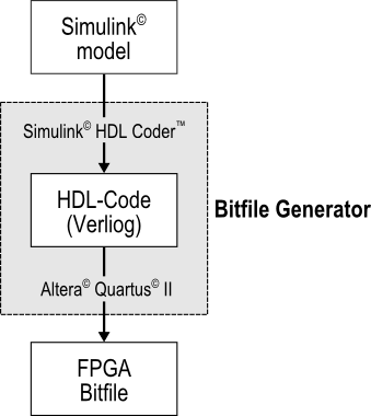
Bitfile Generator
The Bitfile_Generator block is used to generate a custom bitstream for the Altera Cyclone FPGA on the USRP mainboard.
Description
Based on a Simulink model, the Bitfile Generator first produces a HDL-file using the Simulink HDL Libraries and Coder (see Simulink HDL Coder help for more detailed information). Afterwards, the place&route process is performed by the Altera Quartus II Software. The flow graph below shows the whole process. The generated bitfile (*.rbf) can be set using the Set Bitstream block (see help usrp_helper).
Bitfile Generator Build Process
Things to keep in mind
- The ADC streams data with a rate of 64 MSps → You must decrease the data rate with decimators
- The DAC demands for data with 32 MSps and then it interpolates internally by a factor of 4 → You must increase the data rate from the model with an interpolator
- If building own FPGA files, the decimation/interpolation rate at usrp_sink/source has to be configured according to your FPGA model. There are no more error catches.
- The input and output ports of the FPGA model only support 16 bit.